歡迎光臨~泰州巨納新能源有限公司
語言選擇:
 ∷
∷

∷
 ∷
∷


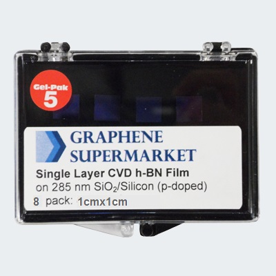
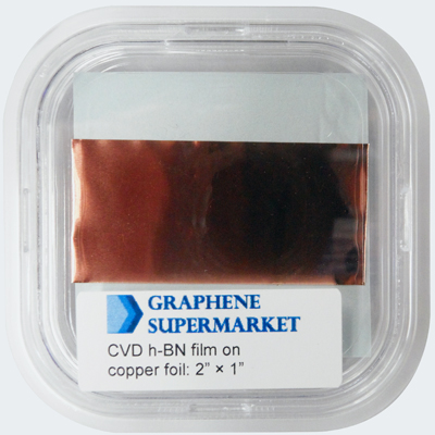
Single layer h-BN (Boron Nitride) film grown in copper foil.
h-BN is an insulator with a direct band gap of 5.97 eV. Due to its strong covalent sp2 bonds in the plane, the in-plane mechanical strength and thermal conductivity of h-BN has been reported to be close to that of graphene. h-BN has an even higher chemical stability than graphene; it can be stable in air up to 1000 °C (in contrast, for graphene the corresponding temperature is 600 °C).
During Chemical Vapor Deposition, BN is grown on both sides of the copper foil
Specifications:
Close to complete coverage (90-95%), with some minor holes
Thickness of the copper foil is 20 microns
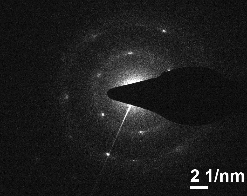
High crystalline quality, see SAD (Selected area [electron] diffraction) data
Quality is confirmed by TEM. TEM shows perfect hexagonal structure.
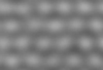
TEM image of perfect hexagonal structure
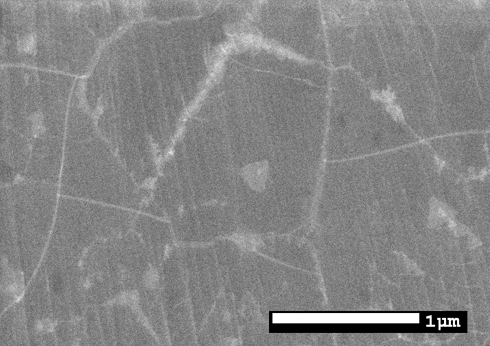
On SEM image (below), BN is seen as wrinkles on top of the copper foil.

SAD data of h-BN
If transferred onto an SiO2 substrate, the BN film may be seen as a white film. However, it is difficult to recognize the BN film on copper using a microscope.

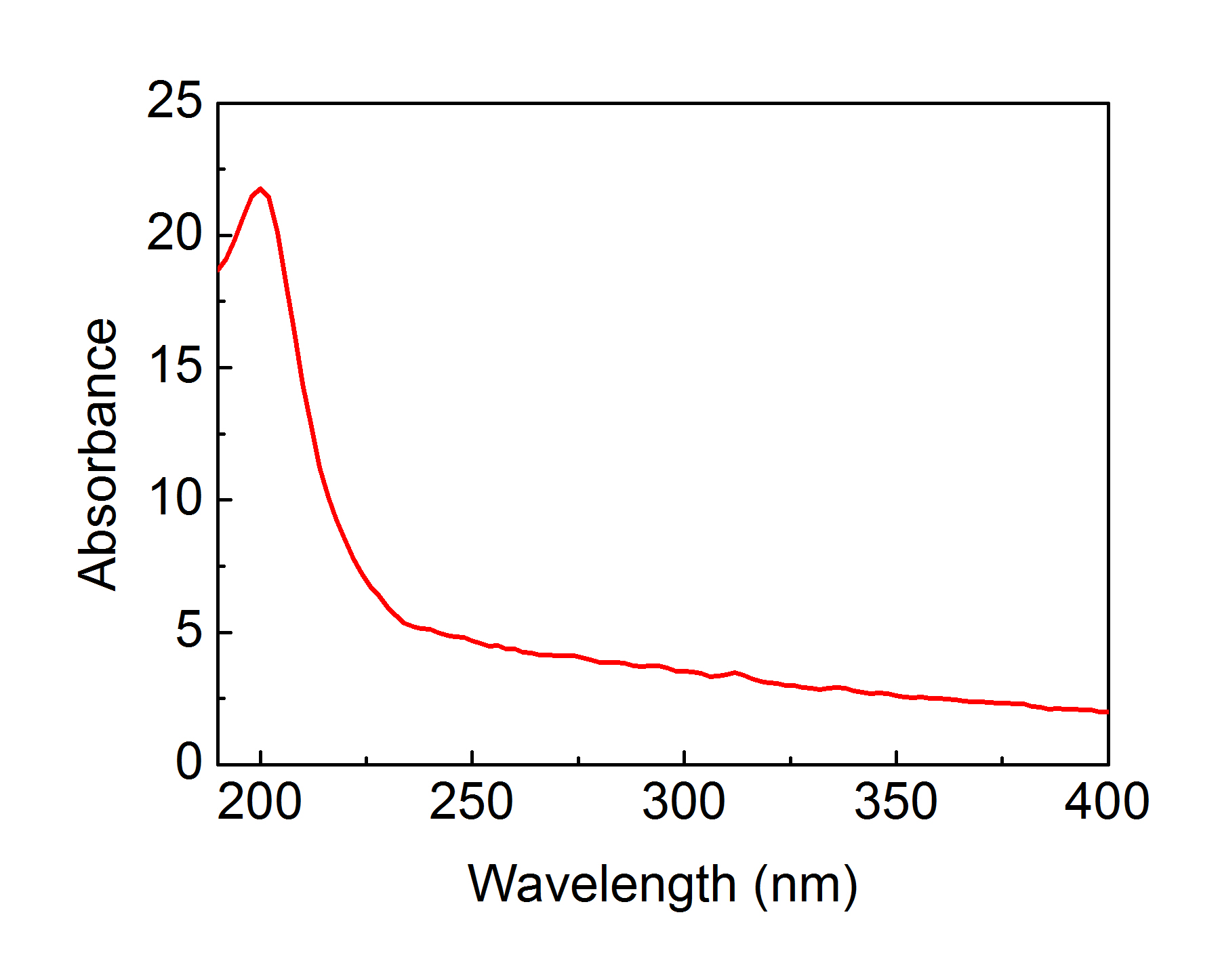
Absorbance data BN on copper
聯系人:嚴春偉
手機:13914543285
電話:0523-86190619,86192878
郵箱:taizhou@sunano.com.cn
地址: 江蘇省泰州市鳳凰西路168號