歡迎光臨~泰州巨納新能源有限公司
語言選擇:
 ∷
∷

∷
 ∷
∷
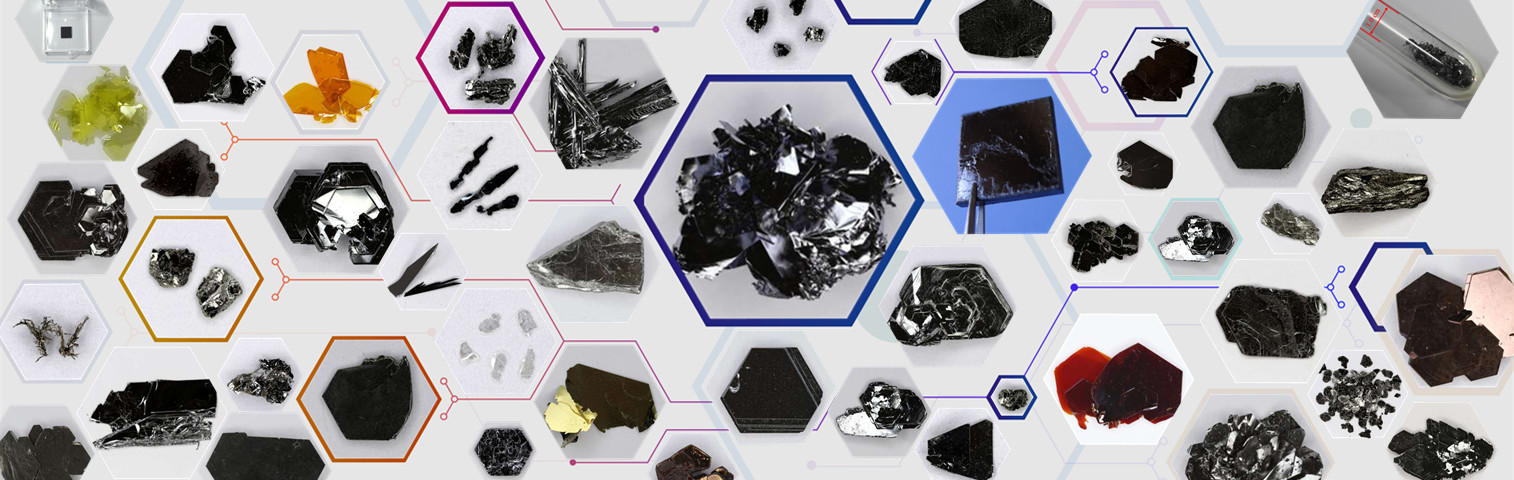


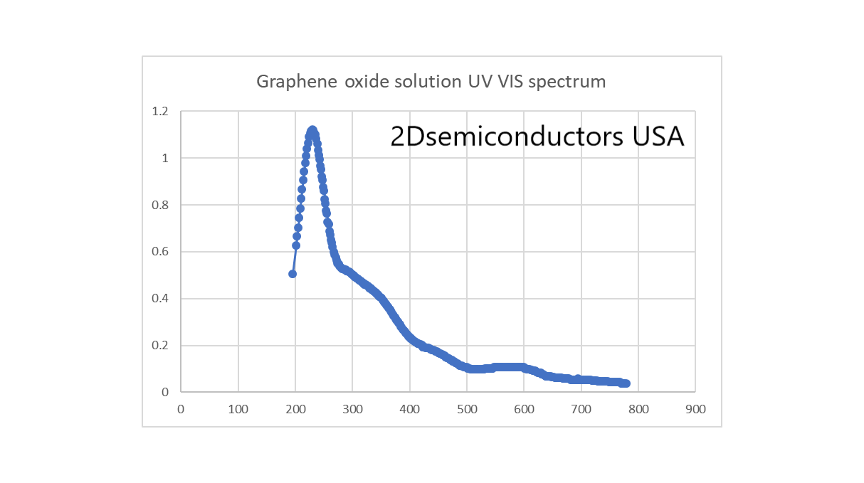

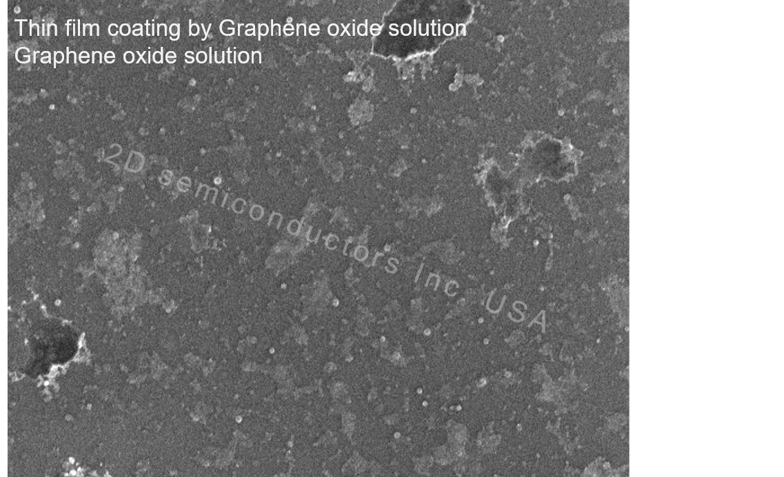
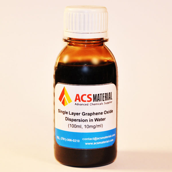
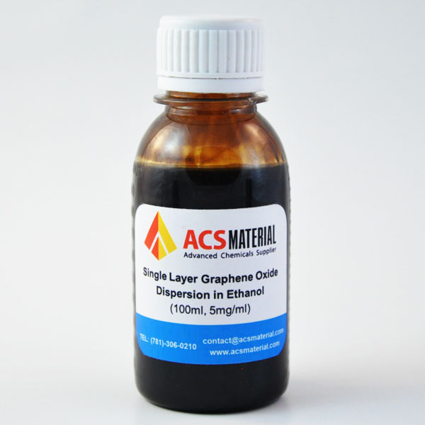
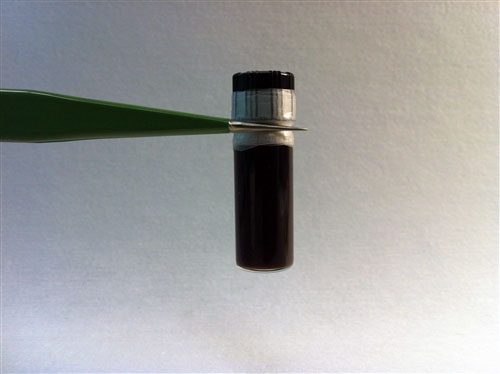
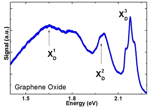
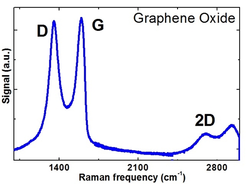
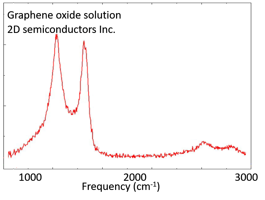
Semiconductor analog of graphene: Graphene oxide has been synthesized at our R&D facilities using modified reaction Hummer technique in water dispersant solution. Growth technique emphasizes on minimizing the defect density to yield optically active material and increasing the average grain size (flake size). Unlike many other graphene oxides, this product is optically active and is ready for 2D semiconductor research. Each growth batch has been characterized by Auger electron and x-ray photoelectron spectroscopy to determine the stoichometry; Raman, PL spectroscopy, and optical absorption for optical properties tests; AFM measurements for the atomic flatness. Product displays PL at ~2.5 eV, sub-bands at 2.2 and 2.0 eV, and broad defect lines at 1.7 eV. Raman spectroscopy measurements yield D, G, 2D, and G+D peaks. Samples come fully saturated with oxygen and the optical properties of the material can be tuned by simple heat treatment. The product is ideal for yielding monolayer onto various substrates within 2-10 minutes. The concentration of monolayer solution is fixed at 92 mg/L.


聯(lián)系人:嚴春偉
手機:13914543285
電話:0523-86190619,86192878
郵箱:taizhou@sunano.com.cn
地址: 江蘇省泰州市鳳凰西路168號