歡迎光臨~泰州巨納新能源有限公司
語言選擇:
 ∷
∷

∷
 ∷
∷

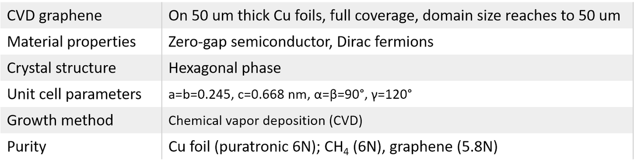
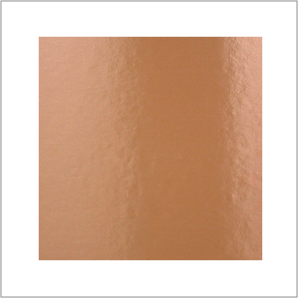
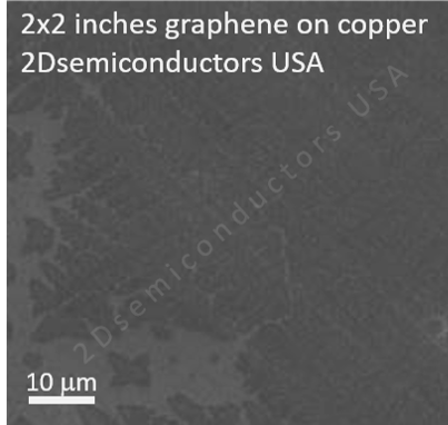
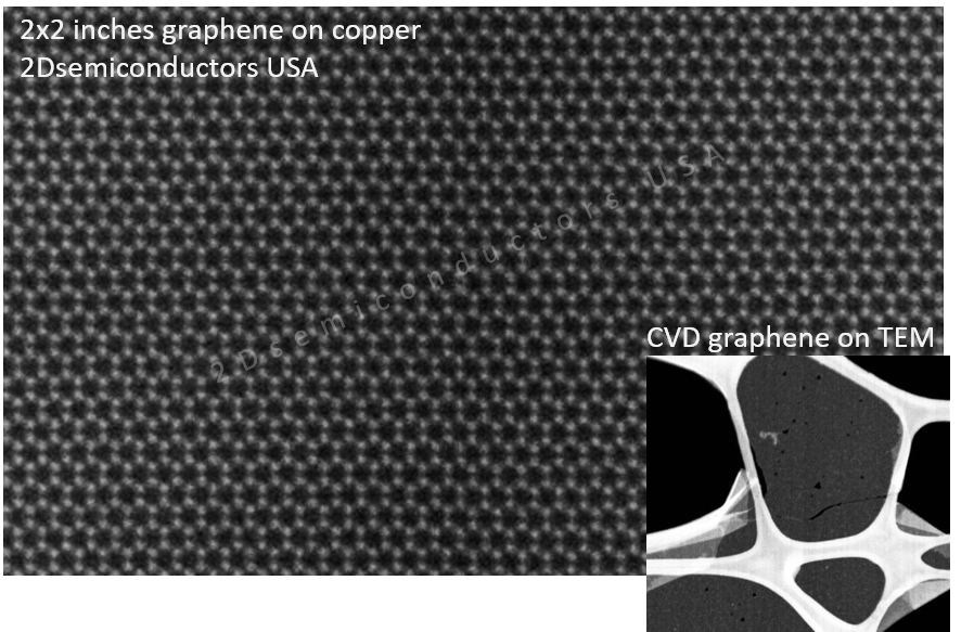
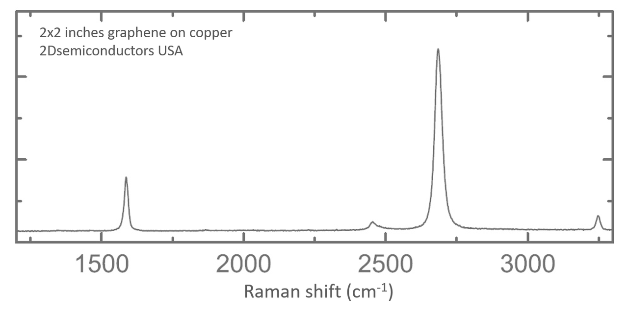
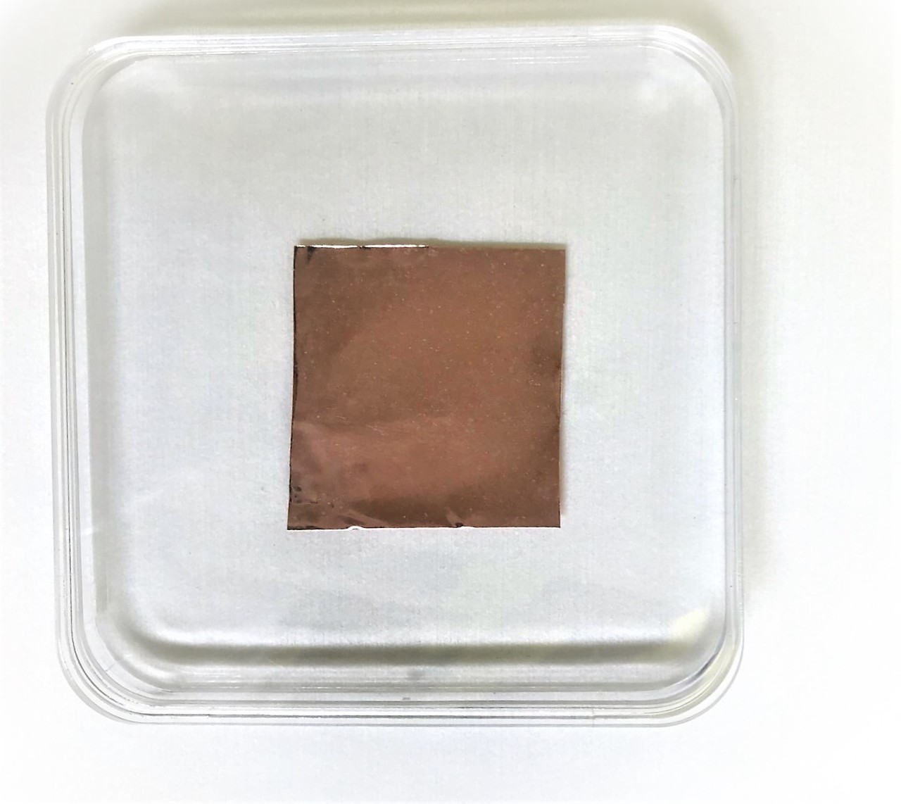
CVD Graphene sheets have been deposited onto 50 micron thick Cu foils using modified chemical vapor technique. In our method, we have paid close attention to engineering defect density and single domain sizes. Most CVD graphene chambers produce small (100nm - 1um) graphene sheets. Our process parameters have been optimized to reduce the point defect (vacancy) concentration, improve crystallinity, increase single domain size, and reduce 1D grain boundary defect density. Our CVD graphene products undergo weekly routine quality control tests to ensure the growth system is accurate and parameters are up to date. Our CVD graphene on copper foils measure 2 inches x 2 inches (~5 x5 cm in size).
If your research needs graphene transferred onto other substrates (SiO2/Si, TEM grids, PET, and other), please contact us for competitive pricing options.
Advantages of CVD graphene on copper foils from 2Dsemiconductors USA
Designed, synthesized, and manufactured in USA. All the constituent precursors are all made in U.S.A and produced at our facilities.
CVD graphene products undergo weekly route characterization tests to ensure parameters are up to date and optimized.
Defect density has been confirmed at 1E8 - 1E9 cm-2 density
Large single domain sizes
Less 1D grain boundary defect density
100% compliance with USA customer protection act
Properties of graphene on copper


聯系人:嚴春偉
手機:13914543285
電話:0523-86190619,86192878
郵箱:taizhou@sunano.com.cn
地址: 江蘇省泰州市鳳凰西路168號