歡迎光臨~泰州巨納新能源有限公司
語言選擇:
 ∷
∷

∷
 ∷
∷


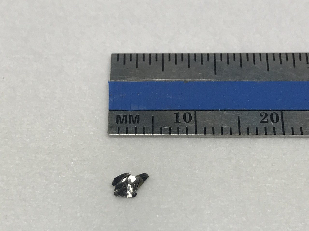
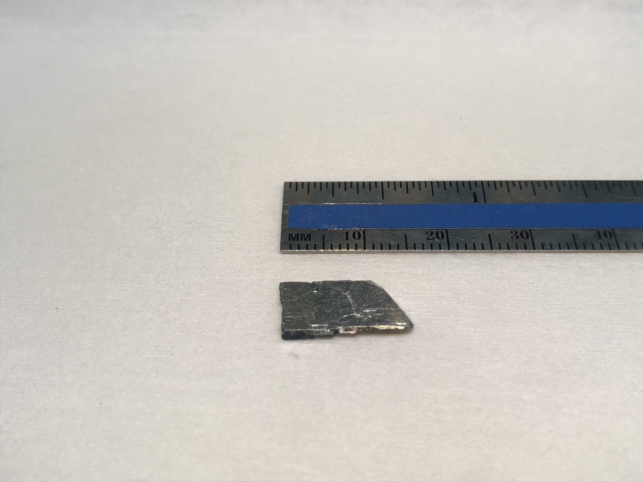
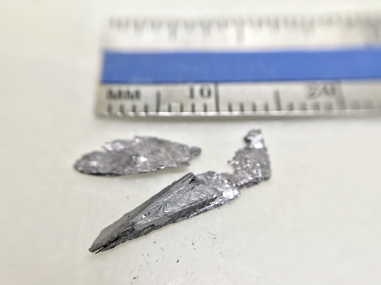
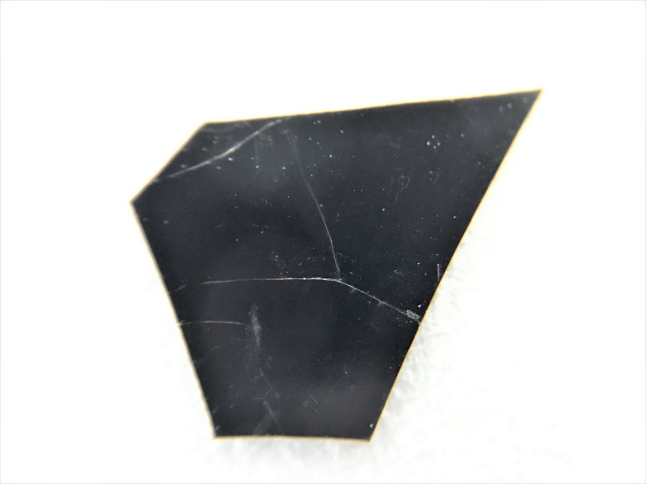
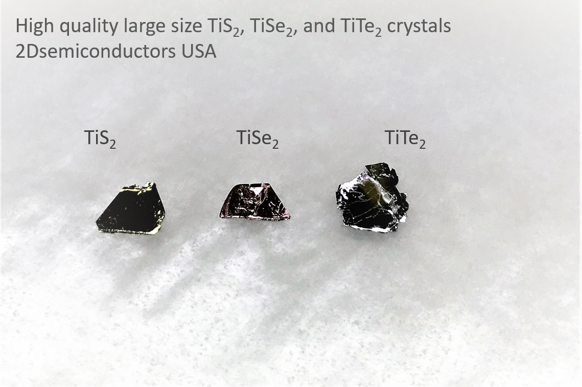
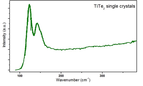
Similar to graphene and MoS2, TiTe? is also layered material (layered transition metal dichalcogenide) crystallizing in the 1T-CdI2 structure. It is a semimetal but very small gap (~50-100 meV) opens up as a result of charge density waves (CDW) formation.Owing to weak interlayer couple can be isolated to monolayers on variety substrates. From few- to monolayers, TiTe? possesses various interesting physical properties ranging from unusual - extraordinary Raman spectra and electrical conductivity. Each sample is characterized by various techniques such as electrical conductivity, Raman spectrum, XRD, XPS, AES, and ARPES to provide the highest quality samples for your research needs.
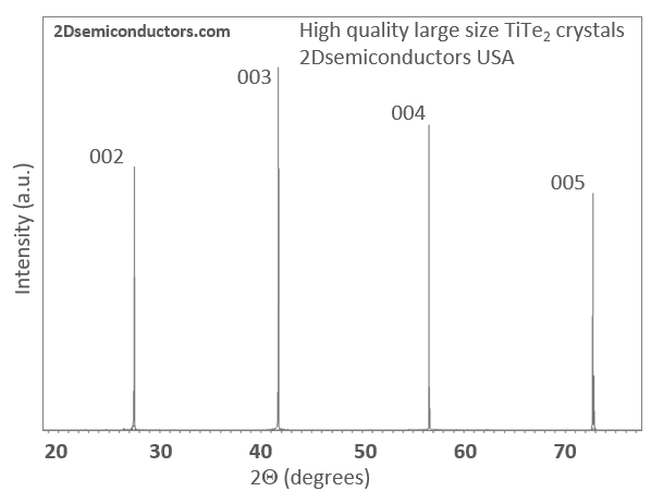
Our TiTe2 crystals are stabilized in 2H-phase (semimetallic and CDW metallic phase). They are grown using two different techniques through chemical vapor transport (CVT) or flux zone growth (see description of these two methods below). These crystals are treated as gold standards in 2D materials field owing to perfected electronic behavior with guaranteed electronic response and low zero temperature resistance values. Our TiTe2 crystals exhibit low impurity resistance (zero temperature resistance), high carrier mobility, extremely clean and sharp XRD peaks, and negligible amount of defects (see published results as well as CVT vs. Flux based methods below ). TiTe2 crystals come ready for exfoliation without any preparation. If you research needs STM grade surfaces or even STM samples (TiTe2 mounted on conductive STM holders) please contact us, we will be happy to arrange these samples.
Properties of vdW TiTe2 crystals
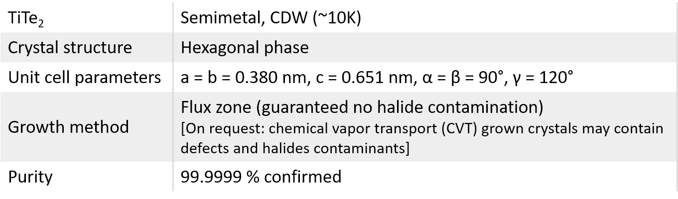
Growth method matters> Flux zone or CVT growth method? Contamination of halides and point defects in layered crystals are well known cause for their reduced electronic mobility, reduced anisotropic response, poor e-h recombination, low-PL emission, and lower optical absorption. Flux zone technique is a halide free technique used for synthesizing truly semiconductor grade vdW crystals. This method distinguishes itself from chemical vapor transport (CVT) technique in the following regard: CVT is a quick (~2 weeks) growth method but exhibits poor crystalline quality and the defect concentration reaches to 1E11 to 1E12 cm-2 range. In contrast, flux method takes long (~3 months) growth time, but ensures slow crystallization for perfect atomic structuring, and impurity free crystal growth with defect concentration as low as 1E9 - 1E10 cm-2. During check out just state which type of growth process is preferred. Unless otherwise stated, 2Dsemiconductors ships Flux zone crystals as a default choice.
聯系人:嚴春偉
手機:13914543285
電話:0523-86190619,86192878
郵箱:taizhou@sunano.com.cn
地址: 江蘇省泰州市鳳凰西路168號