歡迎光臨~泰州巨納新能源有限公司
語(yǔ)言選擇:
 ∷
∷

∷
 ∷
∷

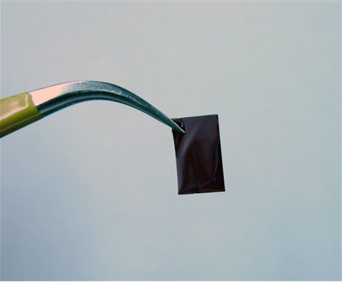

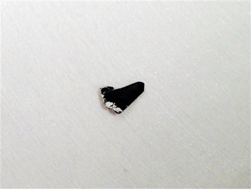
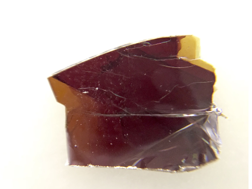
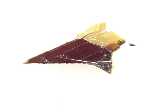
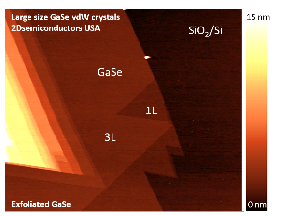
Unlike other sources, our GaSe crystals are best suited towards electronic and optical applications in 2D materials field. Our GaSe (gallium selenide) crystals have been synthesized through three different growth techniques, namely Bridgman growth, chemical vapor transport (CVT), and flux zone growth, to optimize grain sizes and reduce defect concentrations. Large grain sizes and controlled defects enable you to yield monolayers through simple exfoliation process with high yields, get high electronic mobility, and ideal exciton recombination times. By default, 2Dsemiconductors USA provides Bridgman growth GaSe crystals cut in 0001 direction ready for exfoliation. However, if your research needs CVT or flux zone grown GaSe please drop a note during check out.
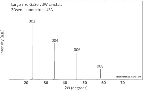
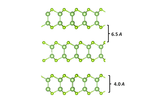
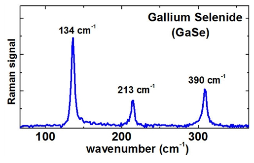
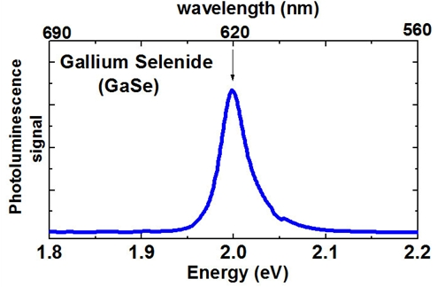
Properties of vdW GaSe crystals - 2Dsemiconductors USA
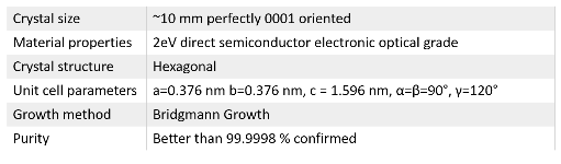
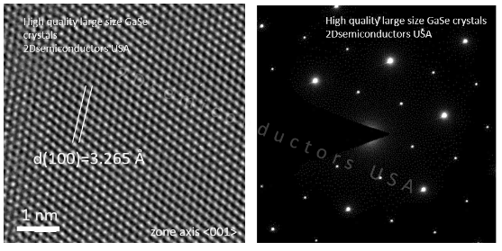

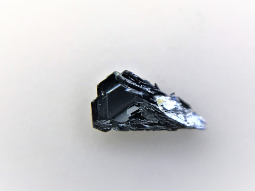
Growth method matters> Flux zone or CVT growth method? Contamination of halides and point defects in layered crystals are well known cause for their reduced electronic mobility, reduced anisotropic response, poor e-h recombination, low-PL emission, and lower optical absorption. Flux zone technique is a halide free technique used for synthesizing truly semiconductor grade vdW crystals. This method distinguishes itself from chemical vapor transport (CVT) technique in the following regard: CVT is a quick (~2 weeks) growth method but exhibits poor crystalline quality and the defect concentration reaches to 1E11 to 1E12 cm-2 range. In contrast, flux method takes long (~3 months) growth time, but ensures slow crystallization for perfect atomic structuring, and impurity free crystal growth with defect concentration as low as 1E9 - 1E10 cm-2. During check out just state which type of growth process is preferred. Unless otherwise stated, 2Dsemiconductors ships Flux zone crystals as a default choice.
1. Journal of Nanoelectronics and Optoelectronics Vol. 7, 1a€“3, 2012
2. ACS Nano, 2012, 6 (7), pp 5988a€“5994
聯(lián)系人:嚴(yán)春偉
手機(jī):13914543285
電話:0523-86190619,86192878
郵箱:taizhou@sunano.com.cn
地址: 江蘇省泰州市鳳凰西路168號(hào)