歡迎光臨~泰州巨納新能源有限公司
語言選擇:
 ∷
∷

∷
 ∷
∷
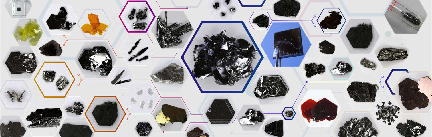


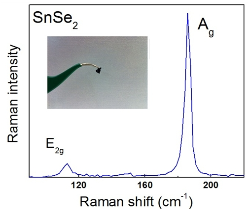

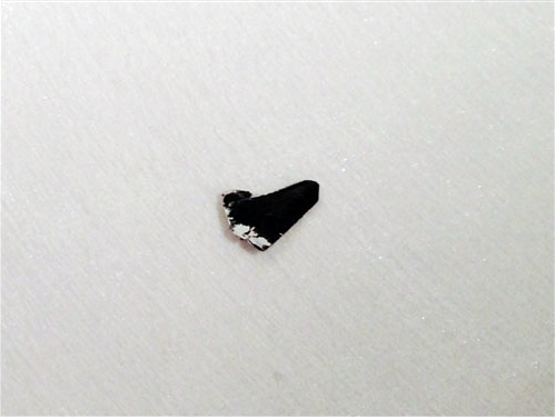
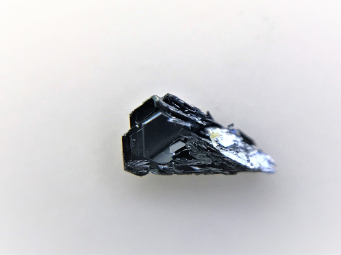
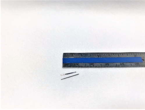
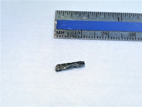
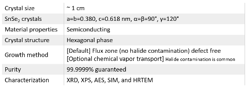
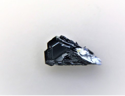
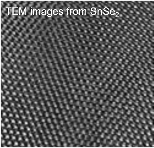
World record size single crystal SnSe? (Tin diselenide) crystals are developed at our facilities using state-of-art techniques. All the crystals are ready to exfoliate as shown in the images. Crystals are larger than 1cm in size giving you plenty of material to work with. In the bulk form SnSe? is 1.0 eV direct band gap semiconductor and becomes 1.4 eV direct semiconductor in the monolayer form. Displays remarkable and unusual optical, mechanical, and electrical properties that are waiting to the published in the literature. Yet, monolayer SnSe? remains unknown by the scientific community and waiting to be discovered. Crystals are highly crystalline with very sharp Raman peak signal at 109 and 182 cm-1 with FWHM less than 4cm-1. They are developed at our facilities using state-of-art flux zone techniques. Each growth takes close to three months to provide you perfected crystals that does not contain any halides. In contrast to commonly used chemical vapor transport (CVT) technique, flux grown crystals are well known for their structural perfection and electronic/optical performance. Each crystal very large in size to last for years, is highly crystalline, oriented in 0001 direction, and easy to exfoliate. Our R&D staff takes characterization dataset in each sample piece to ensure structural, optical, and electronic consistency.
Characteristics of SnSe2 crystals

聯系人:嚴春偉
手機:13914543285
電話:0523-86190619,86192878
郵箱:taizhou@sunano.com.cn
地址: 江蘇省泰州市鳳凰西路168號