歡迎光臨~泰州巨納新能源有限公司
語言選擇:
 ∷
∷

∷
 ∷
∷

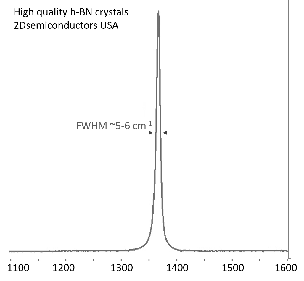
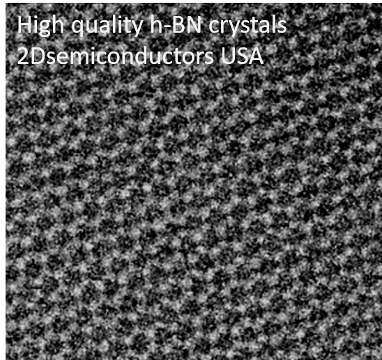
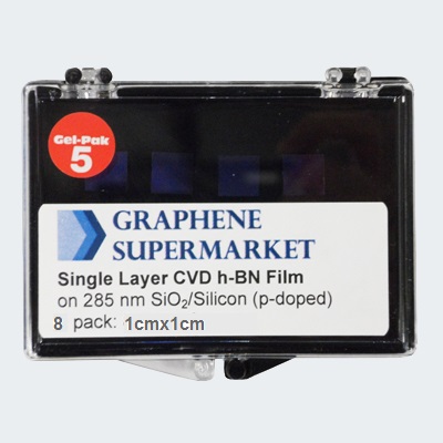
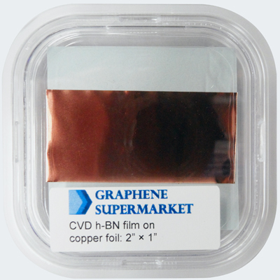
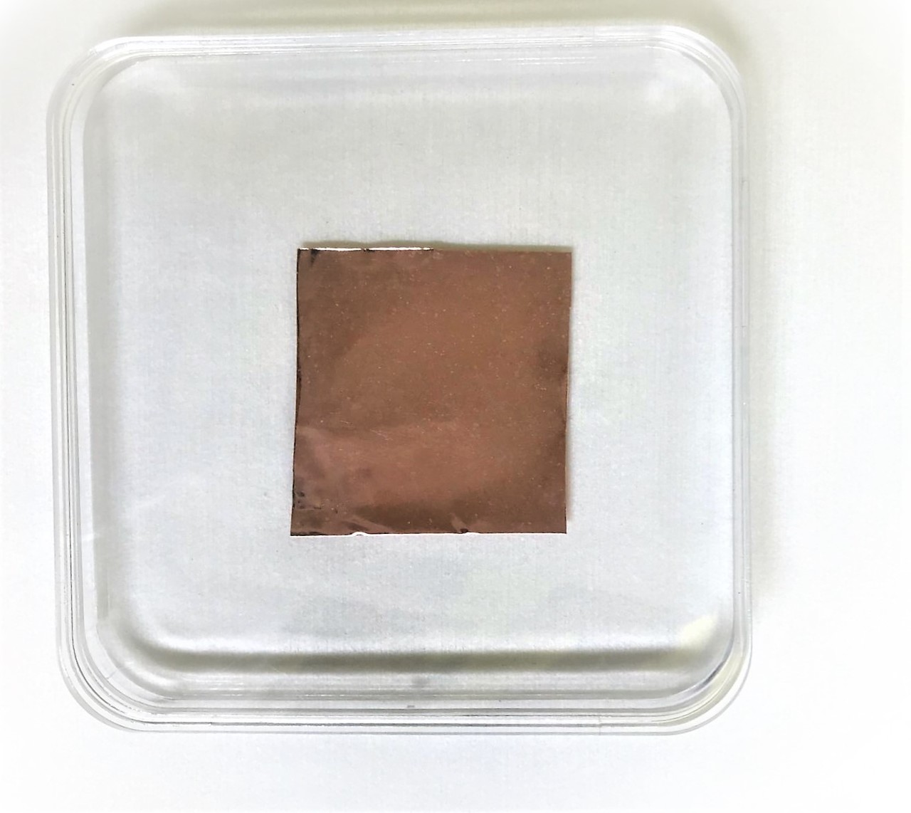
Single layer h-BN (Boron Nitride) monolayer thick film is grown onto 50 um thick copper foils. h-BN is an insulator with a direct band gap of 6 eV with strong ionic bonding between B-N atoms. Our h-BN CVD process has been adopted in order that defect density has been kept low (~1E10-1E11 cm-2) and single domain sizes have been increased to reduce 1D grain boudary defect concentrations. Monolayer h-BN sheets measure ~5cm x 5cm or ~2x2 inches in size.
Properties of h-BN


聯系人:嚴春偉
手機:13914543285
電話:0523-86190619,86192878
郵箱:taizhou@sunano.com.cn
地址: 江蘇省泰州市鳳凰西路168號